Best PCB Designing Course in Chandigarh: Join Best of the Class PCB Designing Course in the region
Every electronic device you touch runs on a Printed Circuit Board (PCB). Think of your phone, laptop, smartwatch, or car dashboard. Skilled engineers design these boards layer by layer and trace by trace. Do you want to learn how these tiny green boards power our world? Now is the perfect time. Learn this craft with our PCB Designing Course in Chandigarh.
A PCB Designing Course in Chandigarh gives you complete hands-on training. You learn schematic capture, component placement, trace routing, and Gerber file generation. Programs at The Core Systems offer offline lab access and expert mentorship. We prepare you for great engineering roles in hardware design and embedded systems.
At The Core Systems, we offer a complete PCB Designing Course in Chandigarh. We build this program for students and working professionals. You get real, job-ready skills. People looking for PCB design training near me choose our offline format. We give you hands-on lab access, direct mentorship, and live projects. Video tutorials cannot match this experience.

Start your career in electronics with our PCB Designing Course in Chandigarh. Expert engineers at The Core Systems teach every class. We have over 25 years of experience building real electronic hardware. Our team has built thousands of real projects for factories and defense. We teach you the exact skills used in today’s electronics industry.
We offer practical lab work and complete job placement support. That makes this program one of the most trusted courses in Chandigarh, Mohali, and Panchkula.
What You Will Learn in This Course
PCB designing turns a circuit drawing into a real physical board. You will learn how to build strong, working circuit boards from start to finish:
-
Placing Electronic Parts: Learn to arrange parts like chips, resistors, capacitors, and connectors neatly on the board.
-
Drawing Safe Copper Tracks: Connect your parts with copper lines. These tracks carry power and signals smoothly without noise or errors.
-
Industrial and Military Standards: Learn to design durable boards. Our methods ensure your boards work in tough factory conditions.
-
Managing Heat and Power: Keep circuits cool by planning wide tracks and proper heat paths for heavy electrical loads.
-
Factory-Ready Files: Create exact manufacturing files like Gerber files and parts lists. Automated factories use these files to build your board.
Course Details
| Feature | Details |
| Training By | The Core Systems (25+ years of experience in hardware and PCB design) |
| Project Experience | Learn from 1,000+ real industrial and military-grade projects |
| Location | Chandigarh (Easy to reach from all Tricity areas) |
| Design Software | Popular tools like KiCad, Altium Designer, and Eagle |
| Job Support | Resume help, interview practice, project portfolio building, and job placement support |
What Is PCB Designing?
PCB designing is the process of creating the physical layout that connects electronic components — resistors, capacitors, microchips, and connectors — using conductive pathways etched onto a board. This layout determines how a device functions, how much power it consumes, and how reliably it performs over time.
 A PCB designer typically works on:
- Schematic capture — drawing the circuit’s logical diagram
- Component placement — arranging parts for optimal performance
- Routing — laying out copper tracks that connect components
- Design rule checks (DRC) — verifying the layout meets manufacturing standards
- Gerber file generation — preparing files for board fabrication
Because nearly every industry — automotive, healthcare, telecom, defense, and consumer electronics — depends on PCBs, the demand for trained designers continues to grow steadily across India, and especially in industrial hubs like Chandigarh, Mohali, and the surrounding Punjab-Haryana belt.
Modern embedded devices, edge-AI nodes, and IoT sensor hubs demand tight integration between compact form factors, wireless RF antennas, and low-noise power supplies. To make you completely versatile, our course delivers in-depth, project-based training across the industry’s top three EDA suites from ground-level basics to advanced multi-layer workflows:
1. Altium Designer (Basic to Advanced)
Altium Designer is the undisputed enterprise standard for high-speed hardware and advanced product engineering.
-
Basic Level: Navigating the unified environment, creating hierarchical schematics, library component creation, and basic 2-layer board layout.
-
Advanced Level: Multi-layer stackup design (4-layer to 8-layer boards), rigid-flex design, interactive length tuning for high-speed buses (DDR, SPI, USB), differential pair routing, 3D clearance checking with STEP enclosures, and automated project release packaging.
-
IoT & Embedded Importance: Essential for developing compact IoT gateways, wearable trackers, and System-on-Module (SoM) boards where tight high-density interconnect (HDI) routing and strict signal integrity are mandatory.
2. Cadence OrCAD PCB Design Solution (Basic to Advanced)
OrCAD is the benchmark across automotive, defense, power electronics, and enterprise industrial equipment.
-

PCB design course in Chandigarh, Mohali, Panchkula Basic Level: OrCAD Capture schematic entry, assigning part properties, basic netlisting, and floorplanning inside OrCAD PCB Editor.
-
Advanced Level: Advanced PSpice analog/mixed-signal circuit simulation, constraint manager configuration for high-speed rules, split-plane power distribution networks (PDN), and EMI/EMC compliance layout practices.
-
IoT & Embedded Importance: Gives you the simulation power to verify complex power supply rails (buck/boost converters) and clean sensor interfaces before ordering expensive prototypes.
3. Autodesk EAGLE (Basic to Advanced)
Autodesk EAGLE remains a beloved industry powerhouse for rapid prototyping, agile hardware startups, and open-source electronics development.
-
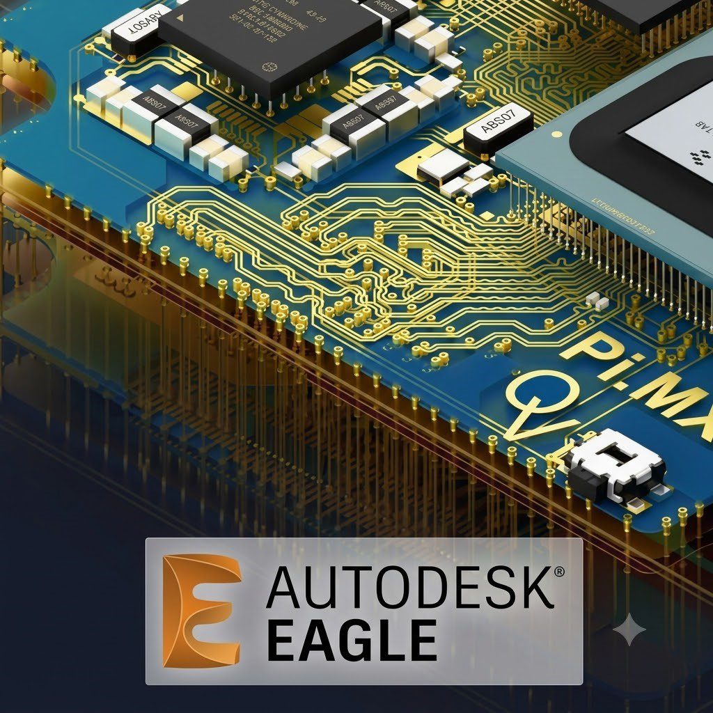 Basic Level: Schematic drawing, custom symbol creation, board layout fundamentals, auto-routing vs. manual routing, and generating basic CAM outputs.
 -
Advanced Level: Writing User Language Programs (ULPs) for workflow automation, managing complex design rule files for specialized board houses, and bi-directional fusion with Autodesk Fusion 360 for seamless electromechanical (ECAD-to-MCAD) enclosure fitment.
-
IoT & Embedded Importance: Ideal for fast turnaround prototyping of smart agriculture nodes, home automation modules, and ESP32/ARM-based connected sensor devices.
 Why Choose The Core Systems for Your PCB Designing Course in Chandigarh
1. Industry-Experienced Trainers
Our mentors are not just academic instructors — they are engineers who have worked on real embedded systems and IoT projects for corporate and industrial clients across Chandigarh, Mohali, Punjab, and Haryana. This means every lesson in our PCB Designing Course in Chandigarh is grounded in practical, current industry practice rather than outdated textbook theory.
2. Offline, Hands-On Learning Environment
We firmly believe that circuit design is a skill best learned by doing. That is why our PCB design course offline structure includes:
- Physical lab sessions with real design software
- One-on-one doubt-clearing with instructors
- Peer collaboration on live design challenges
- Direct access to prototyping tools and testing equipment
Choosing a PCB design course offline over a purely digital format means you get immediate feedback, faster troubleshooting, and a stronger grasp of design fundamentals.
3. Placement-Focused Curriculum
Learning the tools is only half the journey — landing the job is the real goal. Our PCB Design Course with placement assistance ensures you graduate not just with skills, but with a career path. We provide:
- Resume building tailored to embedded/hardware roles
- Mock technical interviews
- Portfolio project development
- Direct referrals to our corporate and industrial partner network in the region
Complete Curriculum: What You’ll Learn in Our PCB Designing Course in Chandigarh
Our program is structured into progressive modules so that beginners and professionals alike can build skills systematically.
Module 1: Fundamentals of Electronics and Circuit Theory
- Basic electronic components and their functions
- Ohm’s Law, Kirchhoff’s Laws, and circuit analysis
- Reading and interpreting datasheets
- Introduction to analog and digital circuits
Module 2: Schematic Design and Simulation
- Creating schematic diagrams using industry-standard software
- Simulating circuit behavior before physical design
- Identifying and correcting logical circuit errors
- Understanding signal flow and component interaction
Module 3: PCB Layout and Routing Techniques
- Multi-layer board design principles
- Trace width and spacing calculations
- Power and ground plane design
- Thermal management basics
- High-speed signal routing considerations
Module 4: Design for Manufacturing (DFM) and Testing
- Design Rule Checks (DRC) and Electrical Rule Checks (ERC)
- Preparing Gerber and drill files
- Understanding board fabrication processes
- Basic testing and debugging of assembled boards
Module 5: Real-World Project Work
Every student enrolled in our PCB Designing Course in Chandigarh completes at least one full project — from concept to a manufacturable design file — under mentor supervision. This project becomes a centerpiece of your professional portfolio.
Module 6: Career Preparation and Placement Support
- Industry-style interview simulations
- Technical portfolio review
- Soft skills and workplace communication training
- Guidance through our PCB Design Course with placement network
Tools and Software You Will Master
Throughout the course, you’ll gain hands-on exposure to widely used PCB design tools common across the electronics industry. Our instructors keep the curriculum updated based on what regional employers are actually asking for, so your skillset stays relevant.

| Skill Area | What You’ll Learn | Industry Relevance |
|---|---|---|
| Schematic Capture | Drawing and validating circuit diagrams | Foundation for all design work |
| PCB Layout | Component placement and trace routing | Core hardware design skill |
| Simulation | Testing circuit behavior virtually | Reduces prototyping errors |
| DFM Practices | Manufacturing-ready file preparation | Required for production roles |
| Debugging & Testing | Identifying board-level issues | Critical for quality assurance roles |
| Documentation | Creating design reports and BOMs | Expected in corporate environments |
Who Should Enroll in This PCB Designing Course in Chandigarh?
This course is designed with flexibility in mind, welcoming a wide range of learners:
- Engineering students (ECE, EEE, Instrumentation) looking to strengthen practical skills before graduation
- Diploma holders seeking a fast-track entry into the hardware and embedded industry
- Working professionals wanting to transition into hardware design roles
- Entrepreneurs and hobbyists developing their own electronic products
- Career switchers from software backgrounds interested in embedded systems
Whether you are a complete beginner or already have some circuit knowledge, our PCB Designing Course in Chandigarh is structured to meet you at your current level and build up from there.
Career Opportunities After Completing the Course
Graduates of our program can pursue several career paths, including:
- PCB Design Engineer — designing layouts for consumer or industrial electronics
- Hardware Design Intern/Associate — supporting product development teams
- Embedded Systems Engineer — working at the intersection of hardware and firmware
- Quality Assurance Technician — testing and validating manufactured boards
- Freelance PCB Designer — offering design services independently to startups and small businesses
With Chandigarh, Mohali, and the broader Punjab-Haryana region emerging as growing centers for electronics manufacturing and industrial automation, local demand for trained PCB designers continues to expand. Organizations such as [Insert link to reputable tech journal/site covering India’s electronics manufacturing growth] have highlighted how India’s push toward domestic electronics production is creating fresh opportunities for hardware talent.
How Our PCB Design Course with Placement Support Works
We understand that many students choose a training program specifically because they want a clear path to employment. That’s why our PCB Design Course with placement track is built around three pillars:
Pillar 1: Skill Certification
Upon successful completion, you receive a certification validating your hands-on proficiency in PCB design — something employers actively look for during technical screening.
Pillar 2: Portfolio Development
You’ll leave the program with at least one completed, presentable PCB design project, giving hiring managers tangible proof of your capabilities rather than just a certificate.
Pillar 3: Direct Industry Connections
Through our corporate and industrial project network across Chandigarh, Mohali, Punjab, and Haryana, we connect capable graduates with companies actively seeking hardware design talent.
Why Offline Training Still Matters in Today’s World
In a world full of online courses, you might wonder why we emphasize an offline PCB design course format. Here’s the honest answer: circuit design is a tactile, detail-oriented skill.
- Immediate error correction: When your routing has an issue, an instructor sitting beside you can point it out instantly.
- Equipment familiarity: Working with actual lab tools builds muscle memory that video demonstrations can’t replicate.
- Peer learning: Classroom discussions often surface problem-solving approaches you wouldn’t discover alone.
- Accountability: A structured, offline schedule keeps learners consistent and motivated.
This is why our PCB design course offline model remains one of the most requested formats among serious learners in the region.
Course Duration, Format, and Eligibility
- Duration: Flexible short-term and extended tracks available to suit students and working professionals
- Format: Fully offline, classroom and lab-based instruction
- Eligibility: Basic understanding of electronics is helpful but not mandatory; beginners are welcome
- Batch Size: Kept intentionally small to ensure personalized mentorship
The Core Systems: Beyond PCB Designing
While this PCB Designing Course in Chandigarh is one of our flagship programs, The Core Systems also provides advanced training across a wide range of in-demand technologies, including:
- Artificial Intelligence and Data Science
- Full-Stack Web Development (MERN and Python with AI)
- IoT and IIoT (Industrial Internet of Things)
- Data Analytics
- Embedded Systems and Python programming
- AWS Cloud Computing
- Cyber Security
- Linux Systems
Many students who complete our PCB Designing Course in Chandigarh go on to combine it with Embedded Systems or IoT training, creating a powerful, hybrid hardware-software skillset that is increasingly valuable to employers across Chandigarh, Mohali, Punjab, and Haryana.
Tips to Get the Most Out of Your PCB Design Training
- Practice consistently: Design skills improve with repetition, not just theory.
- Ask questions early: Don’t let small doubts pile up into bigger confusion later.
- Build side projects: Apply what you learn to a personal project to reinforce your understanding.
- Network with classmates: Many opportunities come through peer referrals and shared learning.
- Stay updated: Follow industry publications to understand emerging PCB design trends and materials.
Conclusion: Start Your PCB Design Career Today
Choosing the right training partner can make all the difference in your career trajectory. Our PCB Designing Course in Chandigarh at The Core Systems combines structured curriculum, experienced mentorship, and genuine placement support to help you transition confidently into the electronics and hardware industry.
Looking for the best PCB design course offline near me in Panchkula, Chandigarh, Mohali, Dera Bassi, or Ambala? Get complete practical lab experience with The Core Systems. We provide a top-rated PCB design course offline with placement support tailored for freshers and working professionals. Visit our Chandigarh campus today, tour our electronics workspace, and see the learning environment for yourself. Your journey toward becoming a skilled PCB designer starts with a single decision — make it today.